|
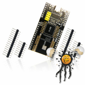
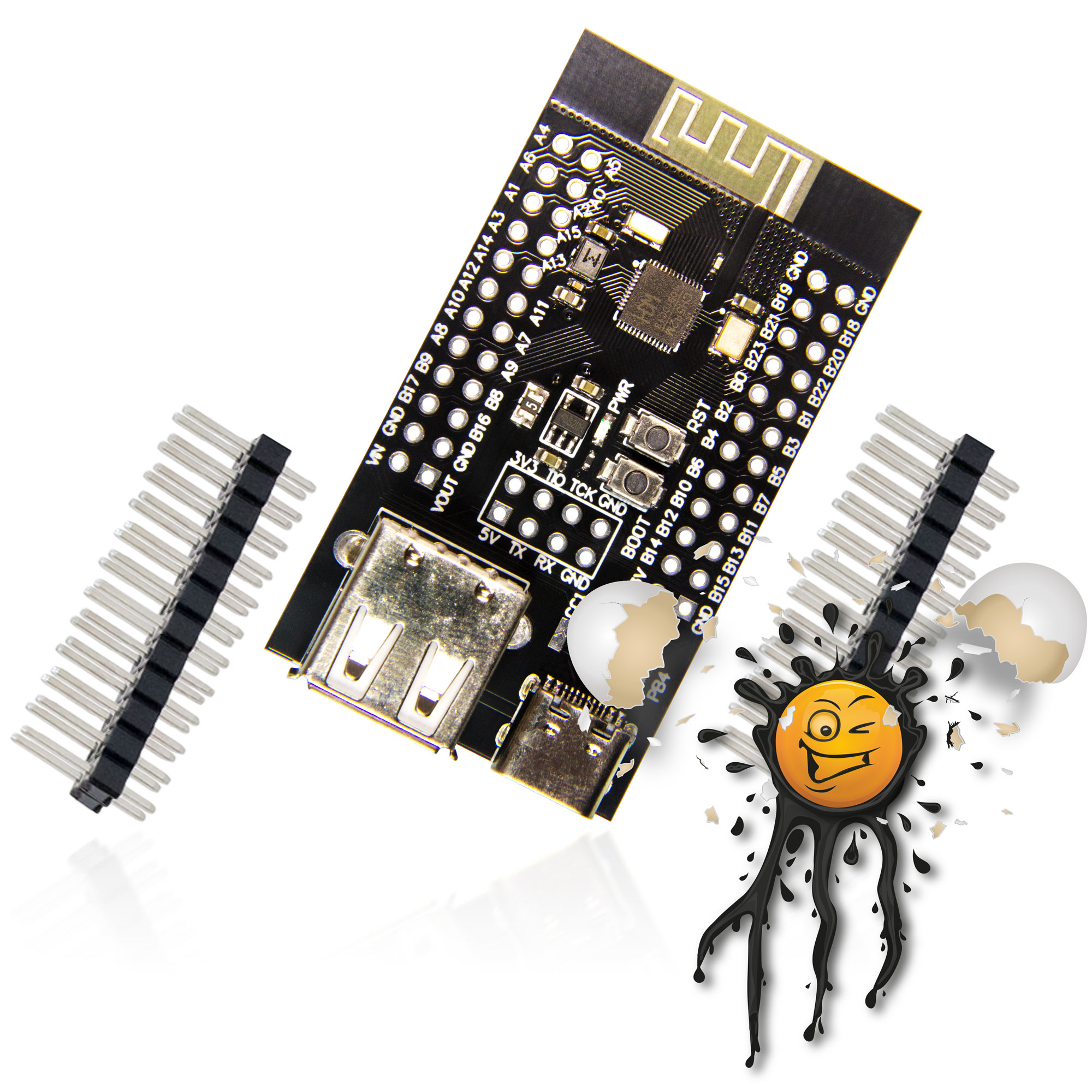
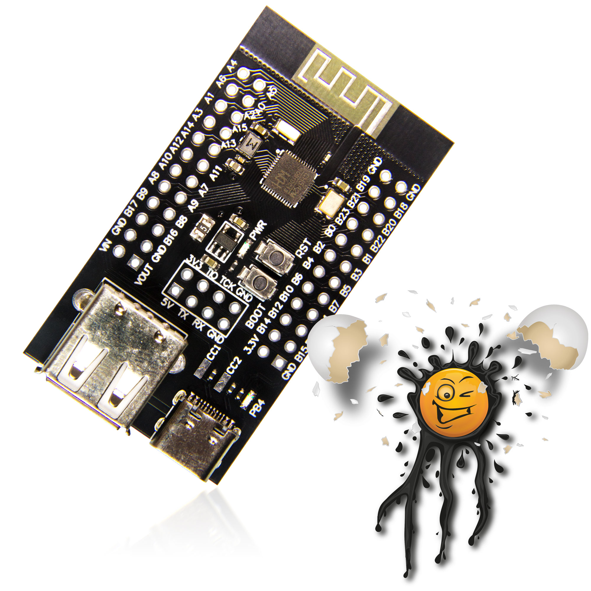
CH582M Bluetooth BLE USB Development Board incl. Pins © androegg
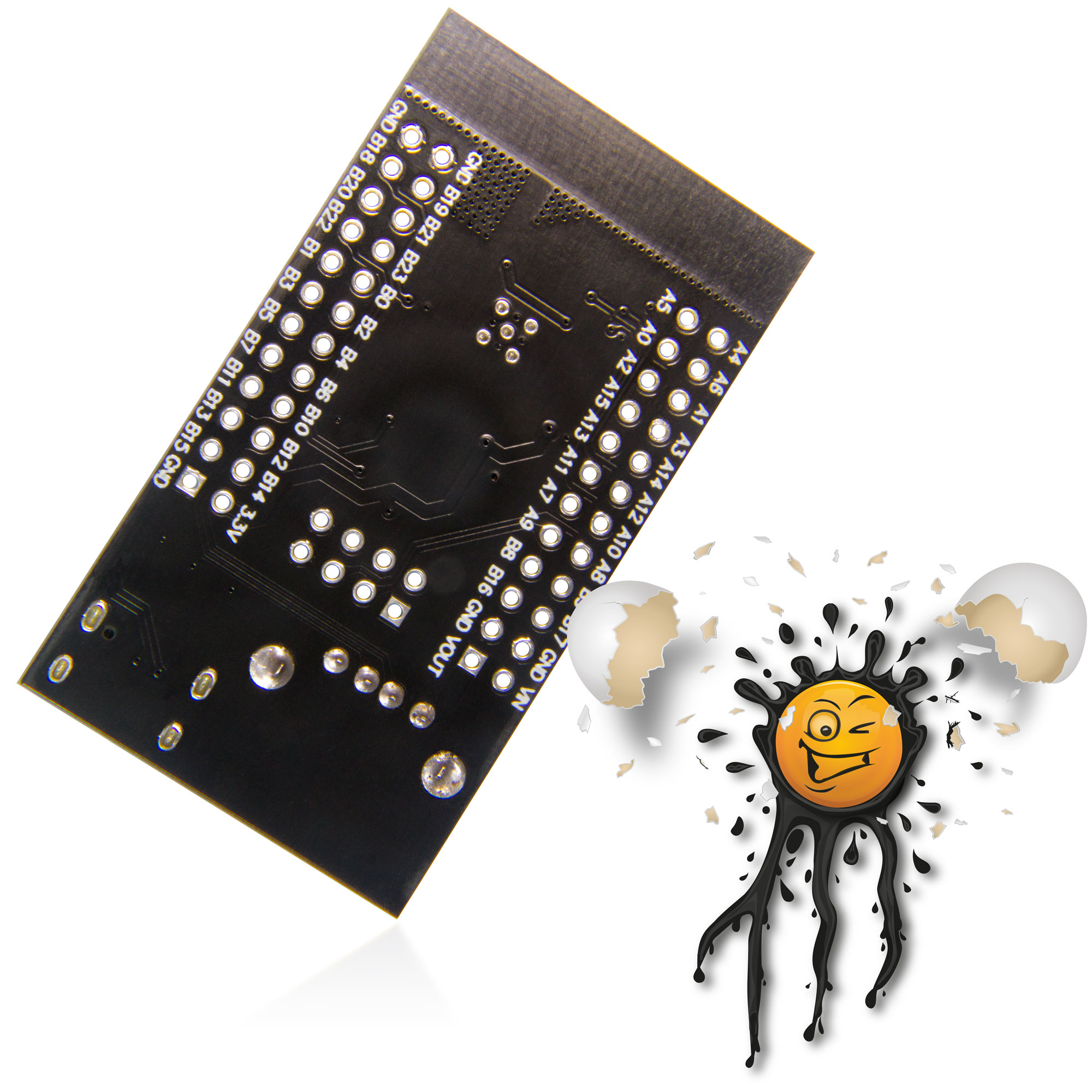
CH582M Bluetooth BLE USB Development Board © androegg
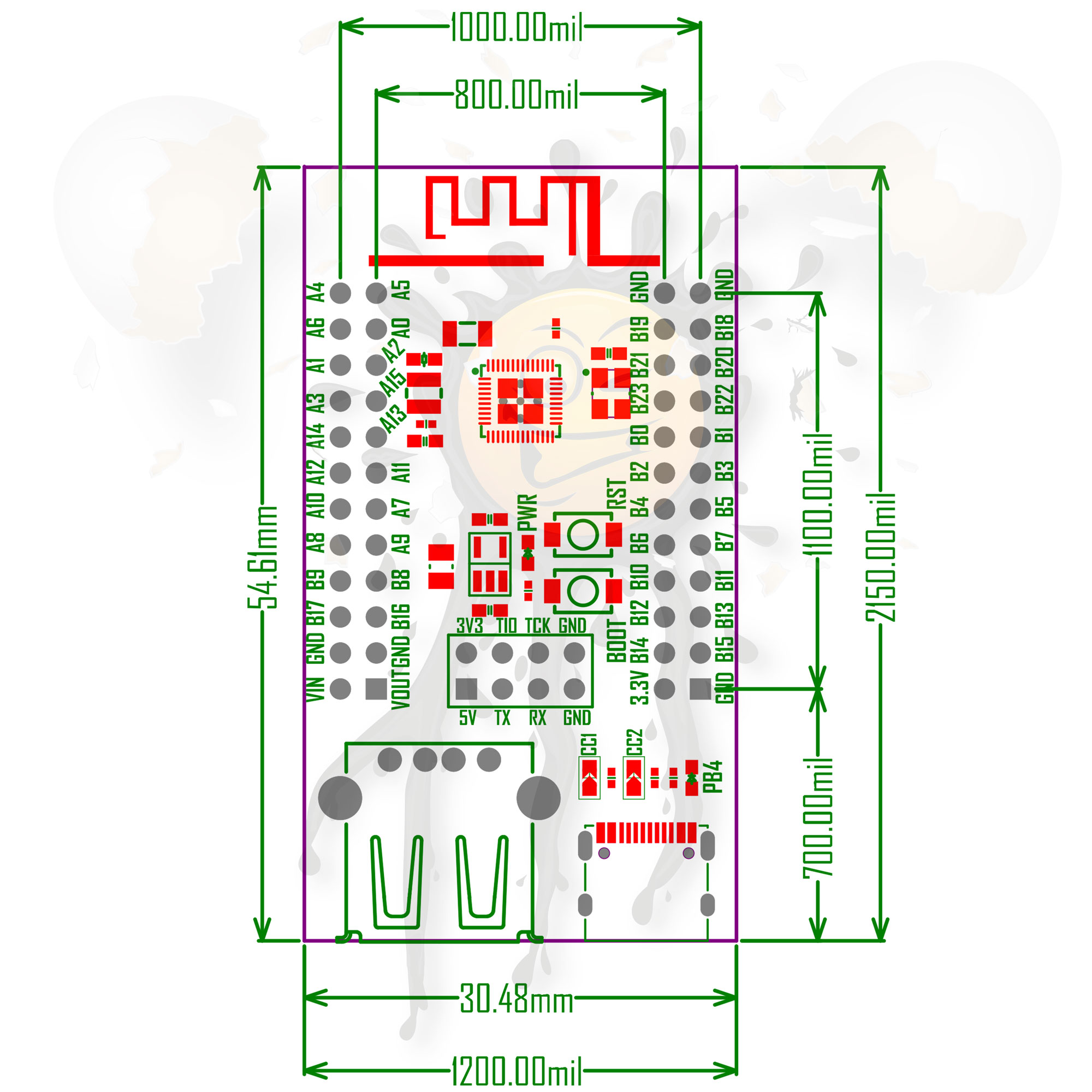
CH582M Bluetooth BLE USB Development Board Dimensions © androegg
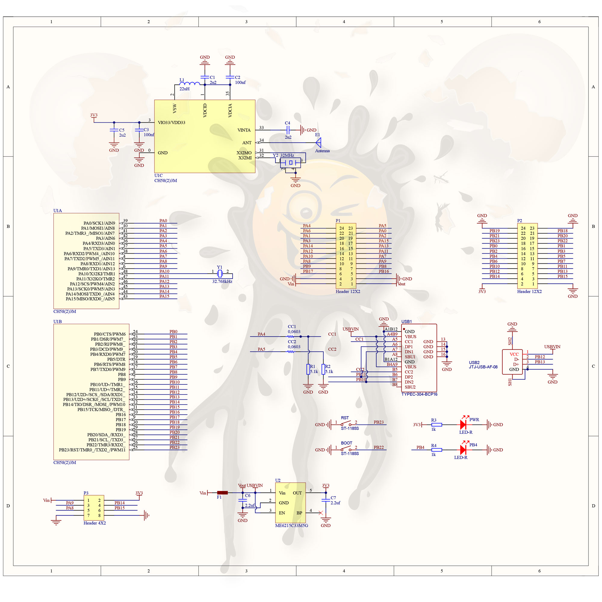
CH582M Bluetooth BLE USB Development Board Schema © androegg
CH582M Bluetooth BLE USB Development Board © androegg
|
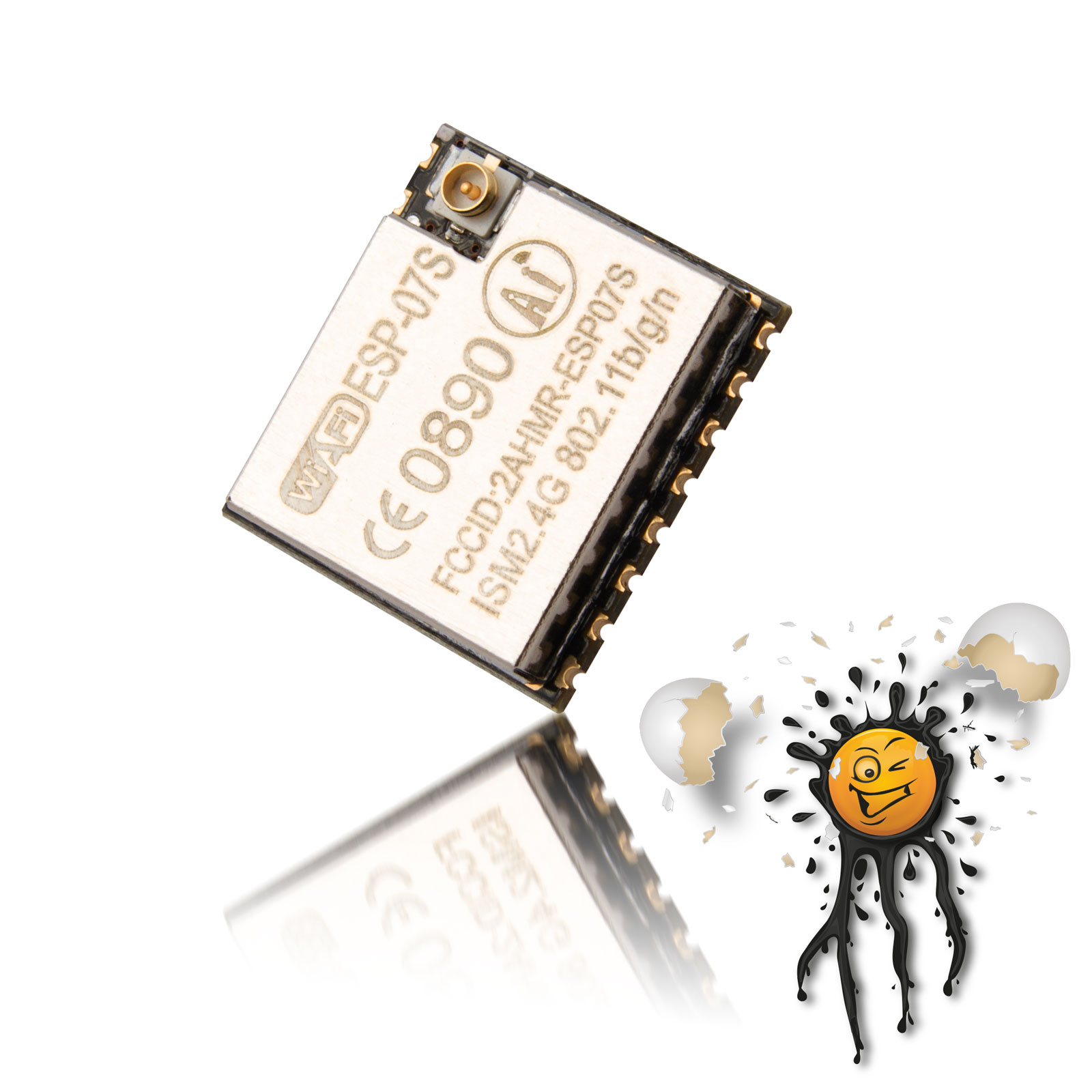
Das CH582M basiert auf einem 32-Bit-RISC-Mikrocontroller und idt optimiert für drahtlose BLE-Bluetooth Kommunikation.
CH582M BLE Entwickler Platine
Der CH582 unterstützt
- 2Mbps Bluetooth Low Energy Kommunikationsmodul
- 2 Full-Speed-USB-Host- und Gerätecontroller und Transceiver
- GPIO
- PWM
- I2C
- SPI
- UART
- ADC
- Touch-Key-Erkennungsmodul
- RTC und andere periphere Ressourcen
|
CH583 is a 32-bit RISC microcontroller integrated with BLE wireless communication.
CH582M BLE Development Board
The chip integrates
- 2Mbps Bluetooth Low Energy communication
- 2 Full-speed USB host and device controllers and transceiver
- GPIO
- PWM
- I2C
- SPI
- UART
- ADC
- touch-key detection module
- RTC and other peripheral resources
|
CH582M Development Board Features:
- Core:
- – 32-bit RISC processor WCH RISC-V4A
- – Support RV32IMAC instruction set, hardware multiplication and division
- -Low-power two-stage assembly line, high-performance 1.56DMIPS
- – Multi-speed system frequency: minimum 32KHz
- – Unique high-speed interrupt response mechanism l
- 512K/1M-bytes non-volatile storage FlashROM:
- – 448KB user application program memory area CodeFlash
- – 32KB user non-volatile data memory area DataFlash
- – 24KB system boot program memory area BootLoader
- – 8KB system non-volatile configuration information memory area InfoFlash
- – Support ICP, ISP and IAP, support OTA wireless upgrade
- – Basically, no waiting at the system frequency of 20MHz l
- 32K-byte volatile data storage SRAM:
- – Sleep retention memory area RAM30K using 30KB dual power supply
- – Sleep retention memory area RAM2K using 2KB dual power supply l
- Power Management and Low Power:
- – Support 3.3V and 2.5V power, CH583M supports 1.8V
- – Built-in DC-DC conversion, reducing power consumption
- – Idle mode: 1.6mA
- – Halt mode: 320uA
- – Sleep mode: Multiple gears from 0.7uA to 2.8uA
- – Shutdown mode: Multiple gears from 0.2uA to 2.3uA
- – Optional low-voltage monitoring of low-power or high-precision battery voltage
- Security properties: AES-128 encryption and decryption, unique chip ID
- Bluetooth Low Energy (BLE):
- – Integrated with 2.4GHz RF transceiver and baseband and link control
- – Receiving sensitivity -98dBm, programmable +7dBm transmission power
- – BLE complies with Bluetooth Low Energy 5.0 specifications
- – Support 2Mbps, 1Mbps, 500Kbps and 125Kbps
- – The wireless communication distance is about 500 meters at the transmission power of 7dBm
- – The communication distance is about 1000 meters at the transmission power of 7dBm and 125Kbps
- – Provide optimized protocol stack and application layer API, and support networking
- Real-time clock (RTC): Support two modes of timing and triggering
- Universal Serial Bus (USB):
- – 2 sets of independent USB controller and transceiver
- – 15 endpoints, support DMA, support 64-byte data packet
- – Integrated USB 2.0 full-speed transceiver PHY, no peripheral required
- – Support host and device mode at full speed/low speed
- Analog to digital conversion (ADC):
- – 12-bit analog to digital converter, support differential and single-ended input
- – 14 external analog signal channels and 2 internal signal channels
- Touchkey detection module (TouchKey): 14-channel
- Timer and Pulse Width Modulation (PWM):
- – 4 sets of 26-bit timers, which can reach 4.2S at the frequency of 16MHz
- – 4-channel capture/sample, support rising edge /falling edge /double edge
- 4-channel 26-bit PWM output, 8-channel 8-bit PWM output
- Universal Asynchronous Receiver/Transmitter (UART):
- – 4 groups of indeoendent UARTs, compatible with 16C550, built-in 8-level FIFO
- – 23-bit counter, communication baud rate is up to 6Mbps
- – UART0 supports some modems, supports hardware automatic flow control
- – UART0 supports automatic matching of slave address during multi-device communication
- Serial Peripheral Interface (SPI):
- – 2 sets of independent SPIs, built-in FIFO
- – SCK serial clock frequency can reach half of system frequency
- – SPI0 supports Master and Slave mode, supports DMA
- Two-wire serial interface (I2C):
- – Support Master and Slave mode, compatible with SMBus
- – Support 7-bit or 10-bit address and bus broadcast
- – Support arbitration, error detection, PEC check and clock extension
- Temperature Sensor (TS)
- Clock: Built-in PLL, built-in 32KHz clock
- General Purpose Input/Output (GPIO):
- – 40 GPIOs, 4 of them support 5V signal input
- – Optional pull-up or pull-down resistor, optional output drive capability
- – 32 GPIOs support level or edge interrupt input
- – 32 GPIOs support level or edge wake-up input
|